
Precision With Nothing in the Way
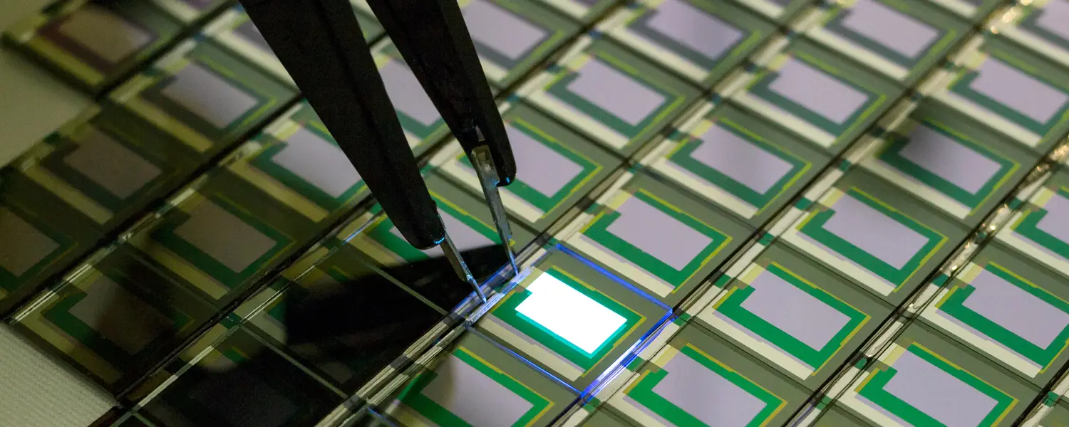
Some of the hardest motion-control problems begin with an apparently simple request, "We need access through the middle."
For life-science imaging, semiconductor inspection, wafer processing, photonics assembly, and laser applications, the ability to illuminate, image, or process a sample from below can be fundamental. Yet creating a large clear aperture through a precision stage removes material from exactly where conventional engineering instinct says stiffness should be added.
That is the open-center paradox.
The aperture creates process freedom, but it can also weaken the structure, reduce rigidity, and make accuracy and repeatability harder to sustain. The challenge is therefore not merely to create a hole in the stage. It is to create an architecture in which the aperture becomes an enabler without becoming an error source.
A successful open-center motion system design must balance aperture size against structural stiffness, bearing placement, load path, and moving mass. Every decision impacts straightness, flatness, orthogonality, and angular behavior at the load point. If the structure flexes or twists as it travels, the sample may be perfectly positioned according to the encoder while being physically misaligned where the imaging or process operation occurs.
In semiconductor wafer inspection, for example, that structural movement can translate directly into a change in the relationship between the wafer and the imaging optics, compromising focus, measurement consistency, or the positional integrity of features being inspected. The aperture therefore has to provide backside access without allowing the stage structure itself to become part of the measurement error.
Bearing selection becomes equally important.
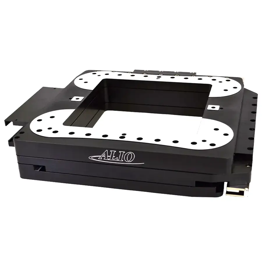
Crossed-roller bearings can provide high stiffness and compact packaging for demanding OEM systems. Air-bearing architectures can offer exceptional smoothness and minimal friction where trajectory quality and geometric performance dominate. Neither option is universally “better.” The correct choice depends on payload, travel, duty cycle, environmental constraints, and the sensitivity of the application to vibration, heat, and angular error.
In high-throughput automated microscopy, for example, smooth trajectory control and rapid settling directly influence how quickly successive fields of view can be captured without degrading image quality. In compact semiconductor or photonics equipment, by contrast, a crossed-roller architecture may provide the stiffness and packaging efficiency needed to maintain alignment while keeping the overall machine envelope under control.
Precision machining and assembly then turn the architecture into a working system. Open-center designs demand tight control of component geometry because small machining or assembly errors can be magnified across the aperture. The stage must not only be built accurately, but it must also be aligned, assembled, and tested as a complete motion platform.
That becomes particularly important in photonics assembly, where an apparently small angular or geometric error in the stage can become a significant displacement at the optical interaction point. In applications such as fibre-to-chip alignment or lens positioning, the quality of the machining and assembly is therefore inseparable from the optical performance the machine ultimately delivers.
That final step is often underestimated.
A datasheet can describe encoder resolution or repeatability, but an open-center system must also prove that it retains rigidity and precision while supporting the real payload, optical path, and process configuration. Verification should therefore include more than isolated-axis performance. It should examine the behaviour of the full stage across travel and under realistic operating conditions.
When engineered properly, an open-center motion system does more than provide backside access. It enables transmitted illumination, dual-sided imaging, through-wafer processing, compact optical packaging, and entirely new instrument layouts without surrendering the precision the application depends upon.
For a digital pathology scanner, that can mean unobstructed transmitted illumination beneath the slide. For semiconductor processing, it can provide access to the wafer from both sides. For laser micromachining or photonics, it can allow the beam path, imaging system, and motion platform to occupy the same tightly integrated working envelope.
At Allient, open-center platforms are designed around this principle: the clearest path through a motion system should not come at the expense of control.